
Nanoscale Characterization & Imaging with Optically Integarted AFM
A Leader in Nanotechnology
Started in 1997, Nanonics Imaging Ltd is one of the most innovative companies in the world in the area of Scanning Probe Microscopy (SPM). This innovation together with unparalleled customer support and collaboration has been the basis of its growth. Today Nanonics has 45 employees in its Jerusalem headquarters and representatives throughout the world.
Nanonics Imaging Ltd has developed a unique and highly differentiated product portfolio in the area of Scanning Probe Microscopy (SPM). Over the last two decades its products have stood at the forefront of technology providing answers for a wide range of nanotechnological applications unavailable with other measurement tools.
Nanonics Imaging Ltd. was the first to realize that the integration of scanning probe microscopes with other standard techniques such as optical microscopy, Raman microprobes, scanning electron microscopes and ion beam microscopes, would introduce critical added value to many of these measurement tools. Thus, its products were developed with such integration in mind and in a variety of these areas it was the first to market such products. It presently has singular and leading offerings in each field.
Breaking Down Barriers for Multiple Probe Operation
Furthermore, Nanonics Imaging effectively overcame barriers that had prevented introduction of scanning multi probe microscopes, SPM systems with more than one probe. It was the first company and is still the only company to have a general multiprobe SPM solution including all forms of SPM measurements such as electrical, thermal, optical, mechanical etc.
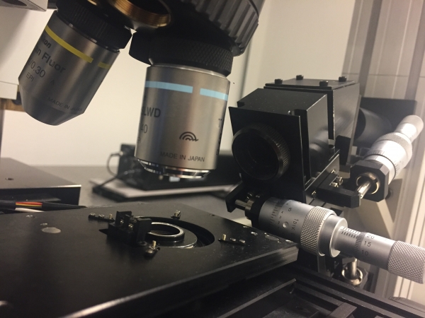
A central development of the company is a novel form of optical microscopy invented by the Founder of Nanonics Imaging, Aaron Lewis. This technique is called Near-Field Scanning Optical Microscopy (NSOM). NSOM is being increasingly recognized as being critical in advancing areas of nano optics and in characterizing plasmonic and photonic devices, optical circuits, advanced opto-electronic components, silicon waveguides and devices and photonic band gap materials and devices.
These nano-optical measurement capabilities even extend to electron and ion beam instrumentation and this has brought super-resolution optical imaging to such areas as cathodoluminescence which have been limited in resolution by far-field optical methods.
Nanotechnology Awards
In each area of its product offerings Nanonics Imaging has won numerous awards over the years. Nanonics Imaging is the proud recipient of the 2015 Microscopy Today Award for the CryoViewMP, the 2013 Microsopy Today award for the AFM-SEM-FIB, the 2010 Microscopy Today award for the Hydra BioAFM, and the 2007 R&D 100 award for the MultiView 4000. These awards cover all areas of microscopic innovation including Raman microprobe integration, multiprobe development, unparalleled scanner advances, forefront probe technologies etc. The company has collaborated with numerous companies such as Renishaw Plc, FEI etc providing SPM solutions that transform the offerings of these partners and allow them to reach new nanotechnological horizons.
NanoTool KitTM of Probes
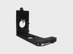
Nanonics has also evolved a NanoTool KitTM of probes that are both multiprobe friendly and do not obscure the optical or the electron/ion optical axis of the microscope. This NanoToolKitTM includes optical, electrical, thermal and even probes providing nanovacuum and nanochemical writing capabilities. These latter probes allow for a unique methodology called NanoFountain Pen Nanochemistry which even permits nanochemical lithography on any surface and with any ink including inks that are gaseous reagents.
With its NanoToolKitTM and its highly differentiated offerings of SPM systems, fully protected by a portfolio of patents, Nanonics has shown great potential to provide measurement capabilities that simply have been unachievable in the past. In essence, the Nanonics Imaging combination of products forms the basis of a variety of measurement technologies that are increasingly becoming an integral component in a penetrating nanotechnological revolution that stands at the forefront of present and future technological revolutions.
Integrating scattering techniques with ultrasensitive SPM/AFM, the SpectraView MV2500 (TM) is a breakthrough in nanochemical analysis: IR-ThZ-Raman-AFM. The SpectraView 2500 (TM) is a compact ultra-low noise scanning probe microscope, offering the highest of resolution and force sensitivity. It offers all modes of AFM, contact, tapping, non-contact and elasticity mapping together with other standard protocols.
Read More Request Quote
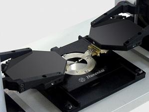
As many as four probes operate simultaneously and independently, with each probe having its own feedback and scanning capabilities. Measure sophisticated properties only possible with the availability of multiple probes such as electrical, thermal and optical properties of devices.
Read More Request Quote
The MultiView 2000 series is an advanced single probe scanning probe microscope enabling a variety of modes of AFM/SPM/NSOM imaging. Nanonics has designed The MultiView 2000 for excellence in scanning probe microscopy while allowing for near-field and far-field optical NSOM/AFM Raman/TERS imaging without perturbation.
Read More Request Quote
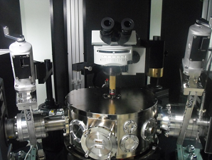
The Cryoview enables measurements of low temperature electrical, optical, magnetic, and thermal properties of materials fully integrated with near-field and far-field optics, Raman, and fluorescence spectroscopies. It opens new avenues for multiprobe measurements including transport properties of materials at temperatures as low as 10K.
Read More Request Quote