Novel Microscopy & Imaging Techniques From Labindia Instruments
At Nano Bio Process Division (NBP), we have been always striving to help our esteemed customers in their research by bringing new advanced and innovative characterization techniques. As optical Microscope is the basic research instruments in any type of Research Lab, one of our idea was to hyphenate microscopy with different other technologies to make systems compatible for cutting edge research.
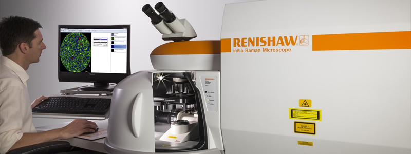
In late 90?s, we brought micro Raman from Renishaw Plc., UK for characterising diamonds where spectrometer was connected to a research grade microscope as a detector & you could get chemical composition from a small volume of 1?m x2?m. The spectrometer had confocality, which allowed depth profiling of upto 2?m. This system could use upto six excitation wavelengths (lasers) and would allow you to record an unstitched spectra over full range. This instrument had a fast imaging facility useful in Pharma, Medical Research etc. We today have almost 130 users of this technique in Industry and academia.
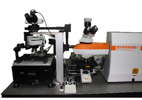
In early 2000 we introduced TERS (Tip enhanced Raman Spectroscopy) by coupling Renishaw Raman with Nanonics AFM. This novel combination opened up many possibilities like AFM-Raman/SNOM-Raman where it pushed the boundary from 1?m to few tens of nanometres for collection of Raman spectra allowing researchers in the field of Nanotechnology achieve mapping and characterisation of their nanocomposites and new materials. At least 15 such users are happily using such hyphenated systems in India. These also include some good life science institutes like IISER Mohali & CCMB Hyderabad.
AFM Raman
Confocal Micro Raman was a misnomer for some researchers who thought they will get two instruments. A good confocal microscope and a Raman spectrometer; our Raman only had a 2?m confocality due to spectrometer pin hole kind of arrangement. However almost 20 years back we did couple a Leica beam scanning confocal microscope with Raman for Unilever Research Centre which allowed them do identification of different layers on soap etc. A similar combination was repeated years later at Birbal Sahani Institute of Palaeosciences at Lucknow with Carl Zeiss confocal microscope allowing them to study fossilized samples.
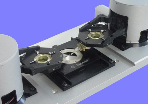
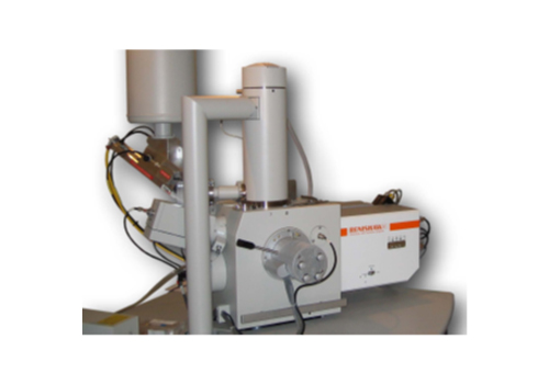
Study of Nanotribology was focused at IISC, Bangalore mechanical engineering department & they were interested in studying self-assembled monolayers which are responsible for friction reduction etc. We therefore connected our Raman with Nano -Tribometer. This was then extended to high temperature & high pressure tribometer for a similar study.
Micro RAMAN TRIBOMETER
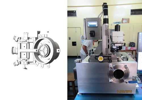
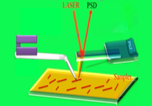
in-situ spectroscopic studies of Friction and wear
- DLC, micro/nanocrystalline diamond
- TiC/a-C, TiN, ZrN, heat treated graphite
- N+ ion implanted steel and reactor grade NiCrB coatings
- @ ambient atmospheric environment & higher temperatures
- To enable correct interpretation of these wear and friction data, and arrive upon appropriate structure-property correlations, is required.
Simple single probe AFM had evolved into a multiprobe AFM at Nanonics which allowed you to observe with one tip while other tip is doing some manipulations such as indentation, deposition, lithography etc. This combination lead to some excellent research from IGCAR Kalpakkam in the area of photonics.
Replacement of feedback beam bounce laser with tuning fork was also an important milestone in improving the images & also in quantifying low forces. This helped in putting TERS on sure footing. Tuning Force feedback also allowed study biological samples immersed in water by avoiding slip to touch due to surface tension of water.
Like Raman, we also connected an FTIR to AFM called it NanoIR which allowed you to collect infrared spectra in nanometre domains, allowing researchers to characterise their nanomaterials.
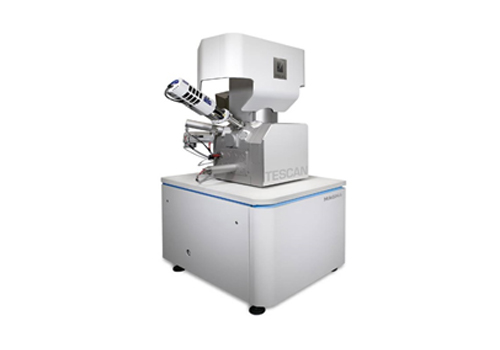
Another important tool is to study and characterise nano materials is scanning electron microscope (SEM). We were lucky to get Tescan range of SEM?s from 1st Dec 2021. Already Tescan has a strong presence in India with around 100 installations. Tescan manufactures all the component such as tubes, sources, detectors, focussing lenses etc. all in house & thus has a better control over the quality of different instruments they make.
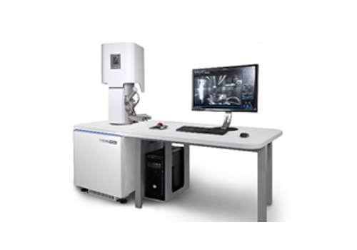
We have thus successfully coupled Raman spectrometer with Research grade optical microscope to confocal microscope, atomic force microscope (AFM), NSOM near scanning optical field microscope and finally also scanning electron microscope (SEM). This then becomes a structure & chemical analyser (SCA). You normally use EDAX on SEM which gives you all the elements in the periodic table but it still does not tell the chemical structure.
Raman gives you possibility to assign a chemical structure thus opening up new possibilities in material characterisations.
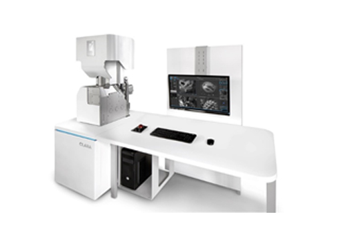
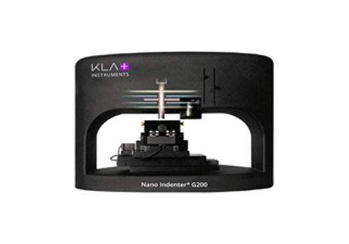
We also have added insitu nano-indentation inside SEM chamber for nano-mechnical characterisation. We have possibility of studying nano-mechanical properties at high temperatures like 800 to 1000Oc.
InSEM HT

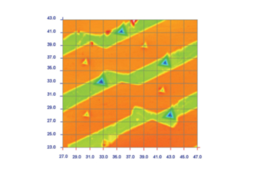
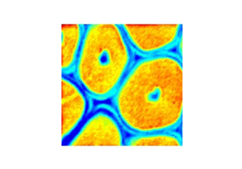
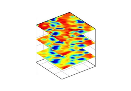
The nano-indentation from KLA can also be used to image & map nano-mechanical properties along Z-axis as a function of depth how various properties such as hardness, stress, strain, elastic modulus changes with respect to depth of penetration can be imaged and quantified.
We will keep adding more such techniques to facilitate and help Indian researchers to be on the forefront.