

WORKSHOP on
Maskless Direct-Write Technologies for the Advanced Micro & Nano-Fabrication
Organized by Heidelberg Instruments in collaboration with Center for Nano Science and Engineering, IISc, Bengaluru
18th Dec 2023 from 09:00 am to 01:30 pm @CeNSE Seminar Hall
About the Workshop:
The workshop aims to bring together experts, researchers, young scientists, and academicians to disseminate knowledge from interdisciplinary backgrounds. The workshop will pro-vide an opportunity to discuss recent developments in Direct Write Lithography research and foster future directions in Nano & Micro device making. The workshop is being organized by Heidelberg In-struments Mikrotechnik GmbH, a pioneer in Direct write maskless lithography Technology developer along with CeNSE, IISc Bangalore. This program offers a forum where you may share compelling key developments in the field of Lithography for R&D and even for Production scale.
| 09:00 AM – 09:30 AM | Registration | |||||
| 09:30 AM – 10:00 AM | Inauguration and Introduction by Prof. Shankar Kumar Selvaraja, CeNSE, IISc-Bangalore | |||||
| 10:00 AM – 10:45 AM | Heidelberg Instruments – Company and Product Overview – Focus on Maskless Aligner and Maskless Stepper by Dr. Sven Preuss Heidelberg Instruments | |||||
| 10:45 AM – 11:15 AM | Empowering microfabrication research with the DWL66+ and unveiling the potential of grayscale lithography by Dominique Collé, Heidelberg Instruments | |||||
| 11:15AM-11:30AM Coffee / Tea Break | ||||||
| 11:30 AM – 12:00 PM | Laser lithography 2D and 3D corrections by Dmitri Titko, GenISys | |||||
| 12:00 PM – 12:30 PM | NanoFrazor Lithography for advanced 2D&3D nanodevices by Vasileios Theofylaktopoulos, Heidelberg Instruments | |||||
| 12:30 PM – 01:00 PM | Talk about Industry Tools/Applications (Focus on MLA 300, ULTRA, VPG) Mask Making by Wolfgang Meixner, Heidelberg Instruments | |||||
| 01:00 PM – 01:30 PM | The MPO 100: 3D Lithography and 3D Microprinting via Two-Photon Polymerization by Dr. Daniel-Alexander Braun, Heidelberg Instru-ments | |||||
| Lunch and Networking | ||||||
Abstracts
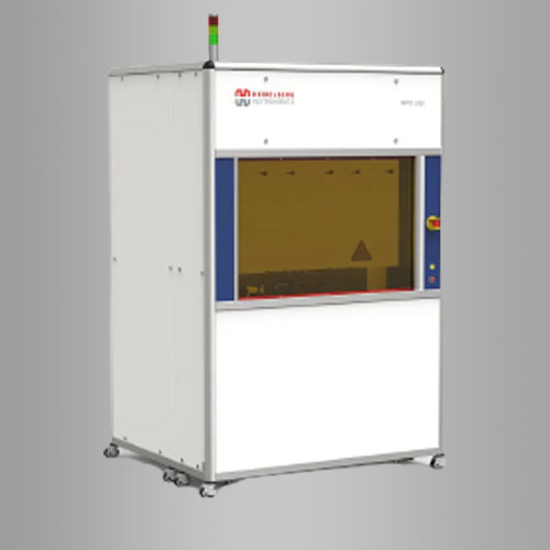
Heidelberg Instruments is a world leader in the design, development, and manufacture of high-precision laser lithogra-phy systems, maskless aligners, and nanofabrication tools. With over 35 years of experience and well over 1,300 systems installed worldwide, Heidelberg Instruments provides lithography solu-tions specifically tailored to meet the micro- and nanofabrication requirements of our global customers.
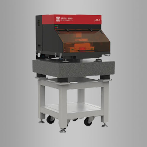
Focus on Maskless Technology (uMLA, MLA 150, VPG 300 DI): When Heidelberg Instruments introduced the Maskless Aligner in 2015, it changed the perception of maskless lithography, and the way lithography is performed in R&D facilities worldwide. This talk will present the features of our established maskless aligners and our new maskless stepper and explain their advantages over traditional mask-based align-ers and steppers.
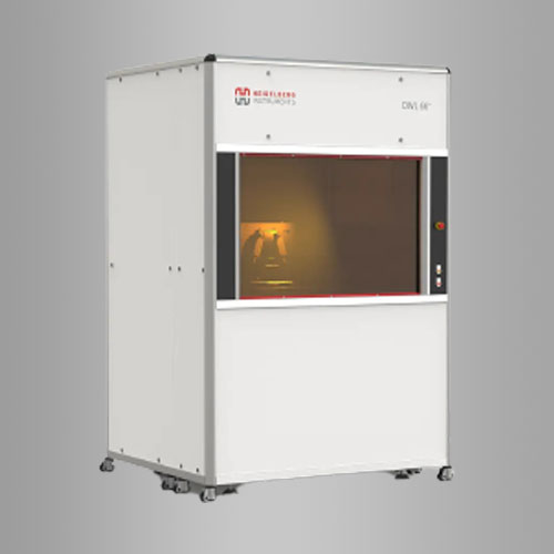
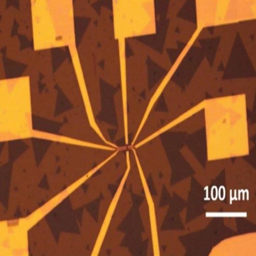
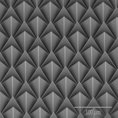
Functioning as an extremely versatile direct lithography tool, the DWL66+ offers the possibility to achieve high resolution (with a minimum structure size of 300 nm) and reach remark able throughput. About 350 of these machines have been installed world-wide. They are employed for a wide variety of needs in educational institutions, research laboratories, and manufacturing sites. Their pri-mary purpose lies in fabricating micro-devices for a diverse array of applications, including microelectronics, sensors, MEMs (Micro-Electro-Mechanical Systems), microfluidics and micro-optics. A sub-stantial portion of the applications served by the DWL66+ revolve around 2.5D micro-optical structures. This is largely attributable to its distinctive ability for direct-write grayscale lithography, a compe-tence for which it is a standard setter.
This presentation will provide overview of CD linearity and shape fidelity correc-tions using OPC provided by BEAMER software, as well as model-based greyscale correc-tions for 3D shapes.
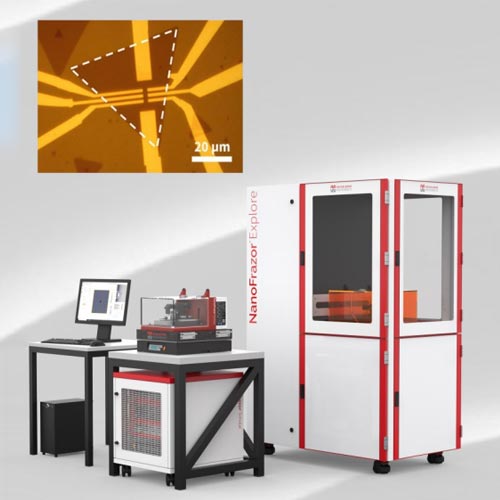
The NanoFrazor technology provides a fabrication platform for nanostructures of arbitrary shapes on a wide range of substrate materials. It uses thermal scanning probe lithography and direct laser sublimation. Thermal nanolithography is achieved through an ultrasharp heated tip. This is combined with in-situ realtime reading of written structures. The writing depth is actively controlled in a closed-loop system. Along with this a laser writer is integrated and can-do mix & match lithography which is helpful to make smaller to bigger structures. Applications range from nanoelectronics, photonics, spintronics to nano-bio arrays.
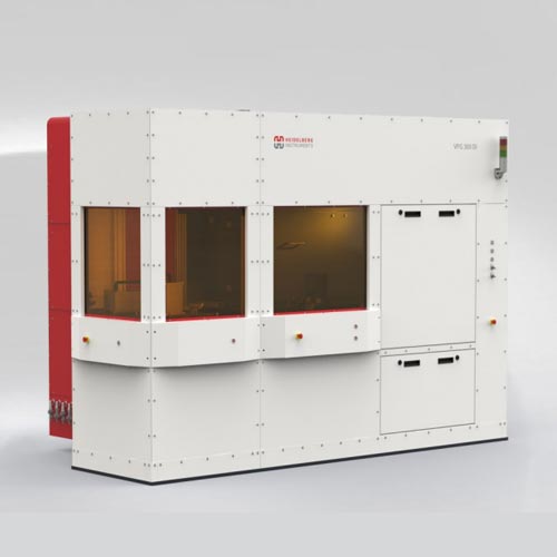
Both throughput and cost of ownership are very important for industrial production. The maskless systems offer significant advantages over mask-based systems such as mask aligners or steppers in terms of flexibility, process results and cost of ownership. With the MLA 300, VPG and ULTRA systems, Heidelberg Instruments has developed machines that are also competitive in terms of throughput.
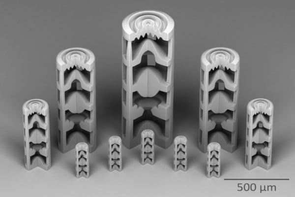
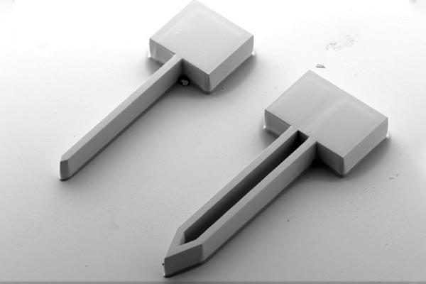
High-precision 3D printing provides a wide range of freedom in design for many applications, like micro-optics, photonics, micro-mechanics and biomedical engineering. The modular 3D printing platform MPO 100 offers high precision on demand for 3D Lithography as well as high print volume for 3D Microprinting and enables production of complex functional microstructures. The talk will give an introduction into the technology and show examples of applications realized with the MPO 100 system.