
Configurable and compact Tabletop Maskless Aligner with Raster Scan and Vector exposure modules

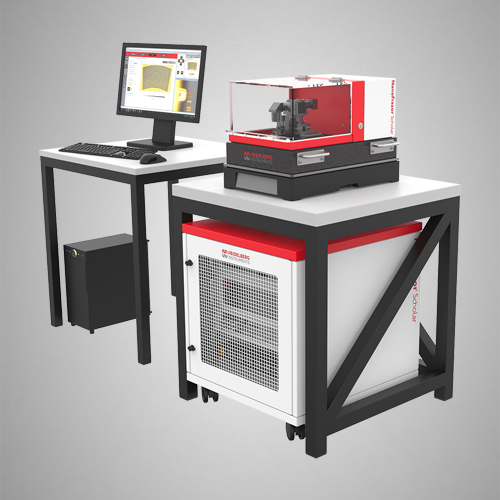
The tabletop µMLA system is state-of-the-art in maskless technology built on the renowned µPG platform – the most sold tabletop maskless system worldwide. It is a perfect entry-level research and development (R&D) tool for virtually any application requiring microstructures. Typical examples are microfluidics (cell sorting devices, lab-on-a-chip), small-scale mask-writing, micro-optics and microlens arrays, sensors, MEMS, contacting 2D materials and fan-out electrodes, etc.
The µMLA is a flexible and customizable tool, and offers two exposure modes. The standard µMLA uses the Raster Scan Exposure Mode for exposures, which is fast and provides excellent image quality and fidelity, while the write time is independent of structure size of pattern density. The optional Vector Scan Mode is designed for patterning continuous smooth curves such as waveguides in a faster and more accurate way. Three optical setups offer a choice of variable resolution and throughput. Each allows easy switching between different resolution and speed configurations to optimize exposure for a given application. The Draw Mode enables straightforward ad-hoc modifications to existing structures and electrical contacts to nanowires or 2D materials. The grayscale exposure mode allows the creation of complex 2.5 structures such as micro-optical devices. With its small footprint, the µMLA fits on a regular table.
Product Highlights :
Direct-write Lithography
No mask-related costs, effort, or security risks
Exposure Quality
Edge roughness raster mode 100 nm; vector mode 30 nm; CD uniformity 200 nm
Exposure Speed
4″ wafer in 90 minutes
Grayscale Lithography
With up to 128 gray levels, the grayscale exposure capability is part of the standard configuration
Small Footprint
640 mm x 840 mm x 530 mm / 25″ x 33″ x 21″ – the smallest tabletop maskless lithography tool
Flexible Configuration
Choice of exposure wavelength; a choice of Raster and Vector Scan Modules
Flexible Use
Software enables easy switching for variable resolution and throughput speeds
User-friendly
Intuitive software and tool operation; easy handling of small samples
Plug-and-play Setup
Simplified plug-and-play installation reduces overall implementation time and saves costs
Available Modules :
Raster Scan Exposure Mode
Fast with excellent image quality and fidelity; write time is independent of structure size or pattern density. LED light source at 365 nm or 390 nm
Vector Scan Exposure Mode
Patterning continuous structures consisting of curved lines – where smooth contours are required. Laser light source at 405 nm and/or 375 nm
Three Optical Setups
Min. resolution of 0.6 µm, 1 µm and 3 µm; variable resolution within each mode
Optional Overview Camera
Fast and easy location of alignment marks or other features of interest on substrate
Glovebox Integration
Glovebox for patterning of sensitive materials in a controlled Nitrogen environment
Draw Mode
Import and overlay of BMP files on top of the real-time microscope image — as in a virtual mask aligner; simple lines and shapes can be drawn into the real-time camera image for immediate exposure
Optical Autofocus
Perfect exposure of small samples (<10 mm)
Exposure Area
Can be upgraded from 100 x 100 mm2 to 150 x 150 mm2
Choice of Exposure, Wavelength and Source
Raster Scan Mode: LED light source at 365 nm or 390 nm. Vector Scan Mode: Laser light source at 405 nm and/or 375 nm
Technical Data
| Write Mode I * | Write Mode II * | Write Mode III * | ||||
| Writing performance (Raster Scan Exposure Module) | ||||||
| Minimum structure size [μm] | 0.6 | 1 | 3 | |||
| Minimum lines and spaces [μm] | 0.8 | 1.5 | 3 | |||
| Address grid [nm] | 20 | 50 | 100 | |||
| CD uniformity [3σ, nm] | 200 | 300 | 400 | |||
| 2nd layer alignment over 5 x 5 mm² [nm] | 500 | 500 | 1000 | |||
| 2nd layer alignment over 50 x 50 mm² [nm] | 1000 | 1000 | 2000 | |||
| Write speed | with 390 nm LED / 365 nm LED | with 390 nm LED / 365 nm LED | with 365 nm LED | |||
| Write speed | 10 mm²/min at 0.6 µm | 40 mm²/min at 1 µm | 100 mm²/min at 3 µm | |||
| Optional write speeds at different minimum structure sizes with “Variable Resolution for Raster Scan Exposure Module” | 18 mm²/min at 1 µm | 60 mm²/min at 2 µm | 120 mm²/min at 4 µm | |||
| 25 mm²/min at 2 µm | 90 mm²/min at 4 µm | 240 mm²/min at 6 µm | ||||
| Writing performance (Vector Mode Exposure Module) | ||||||
| Minimum feature size [µm] | 0.6 | 1 | 3 | |||
| Address grid [nm] | 20 | 20 | 20 | |||
| 2nd layer alignment over 5 x 5 mm² [nm] | 500 | 500 | 1000 | |||
| 2nd layer alignment over 50 x 50 mm² [nm] | 1000 | 1000 | 2000 | |||
| Maximum linear write speed in Vector Mode | 200 mm/s | 200 mm/s | 200 mm/s | |||
| Available spot sizes in Vector Mode [µm] | 0.6 / 1 / 2 / 5 / 10 | 1 / 2 / 5 / 10 / 25 | 3 / 5 / 10 / 25 /50 | |||
| System specifications | ||||||
| Maximum substrate size | 6″ x 6″ | |||||
| Minimum substrate size | 5 x 5 mm2 | |||||
| Substrate thickness | 0.1 to 12 mm | |||||
| Maximum write area | 150 x 150 mm2 | |||||
| Raster scan exposure module | Vector exposure module | |||||
| Light source | LED; 390 nm or 365 nm | Laser; 405 nm and/or 375 nm | ||||
| System dimensions (lithography unit) | ||||||
| µMLA | Width x Depth | Height x Weight | ||||
| Main system housing | 640 mm (25") x 840 mm (33") | 530 mm (21") x 130 kg (285 lbs) | ||||
| Installation requirements | ||||||
| Electrical | 230 VAC / 6A or 110 VAC / 12A (±5%, 50/60 Hz) | |||||
| Compressed air | 6 - 10 bar | |||||
| Cleanroom | ISO 6 recommended | |||||
| Temperature stability | ±1 °C | |||||
| * Only one write mode can be installed on the system | ||||||