
3D Direct-Write Maskless Nano & Micro Lithography Tools
Heidelberg Instruments is a world leader in the design, development, and manufacture of high-precision laser lithography systems, maskless aligners, and nanofabrication tools.
With over 35 years of experience and well over 1,300 systems installed worldwide, Heidelberg Instruments provides lithography solutions serving the global photolithography community in both the direct writing field and in photomask production. Industry stakeholders, as well as working groups of the most renowned universities and research institutes all over the world use Heidelberg Instruments’ systems for the advanced micro- and nanopatterning. Application areas include micro-optics and microsystems technology, photonics, electronics, sensors, semiconductors/advanced packaging (3DIC), quantum computing, MEMS/NEMS, micro-mechanics, biomedical engineering, 2D materials, IoT, and many more.
In the Process and Application Labs (PAL) located in Germany, Switzerland and China, the engineers train and collaborate with customers to make the most of their Heidelberg Instruments equipment.
Based on the extensive know-how in developing customized lithography solutions in the upper mentioned industries and applications fields, Heidelberg Instruments support the customers from the very first design idea, via prototyping and small pilot series to industrial volume production. Extensive services are provided both to the state-of-the-art technology systems and throughout the entire life cycle of older systems.
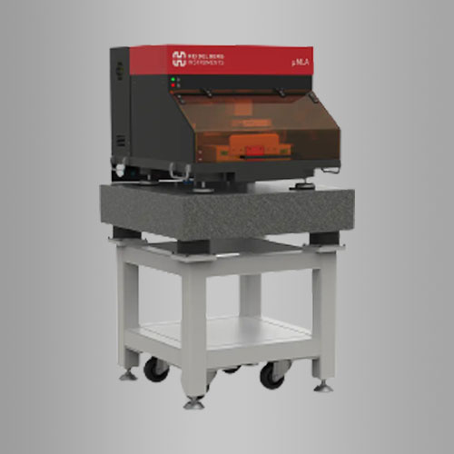
The tabletop µMLA system is state-of-the-art in maskless technology built on the renowned µPG platform – the most sold tabletop maskless system worldwide. It is a perfect entry-level research and development (R&D) tool for virtually any application requiring microstructures.
Read More Request Quote
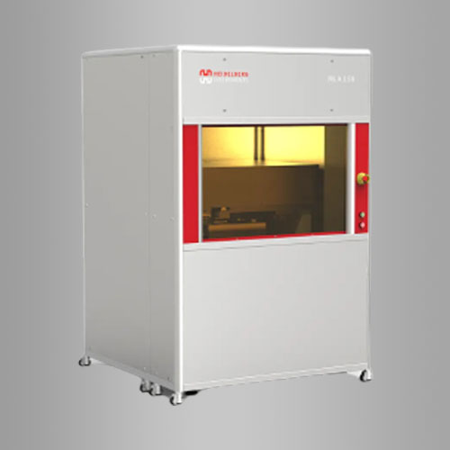
The Maskless Aligner MLA 150 is a state-of-the-art maskless lithography tool. Areas of application include nanofabrication of quantum devices (2D materials, semiconductor materials, nanowires, etc.)
Read More Request Quote
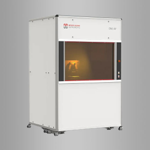
The DWL 66+ laser lithography tool is a high-resolution direct-write pattern generator. As an allrounder, the DWL 66+ is ideal for research and development (R&D) in microelectronics, MEMS, microfluidics, sensors, non-standard substrates, advanced packaging — virtually any academic application that requires microstructure fabrication.
Read More Request Quote
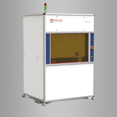
The MPO 100 is a Two-Photon Polymerization (TPP) Multi-User Tool for 3D Lithography and 3D Microprinting of microstructures with applications in micro-optics, photonics, micromechanics and biomedical engineering.
Read More Request Quote
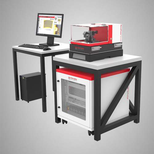
The NanoFrazor® Scholar is the entry level NanoFrazor® system and is particularly suited for academic research groups looking for an easy way to create high-resolution nanopatterns or devices. The NanoFrazor® Scholar is a compact system designed to fit in the smallest lab spaces.
Read More Request Quote
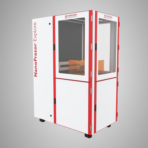
The NanoFrazor® Explore performs with maximum speed, precision and reliability. The technology behind the system is the result of more than 20 years of intensive research and development that started at IBM Research in Zurich and has been extended at SwissLitho and Heidelberg Instruments.
Read More Request Quote